Shortly after I took possession of the MOXF-6 I succumb to the urge to take a look inside. It was an easy job to disassemble the casing unlike the older SY series where the casings are littered with screws of different sizes. I found the build quality of the MOXF-6 just wasn’t up to the same standard as the older SY series, but the board doesn’t suffer anything for this and is still one of the best bang-for-buck boards out there.
Anyways, I’ve posted a few photos of what I found in the MOXF-6. These may help if you ever need to fault-find, compare, or just to save you the task of opening your own if you are curious to see what’s inside.
I have made some comments regarding the ICs and the functions of the PCBs but please don’t take these as 100% correct, or even 50%😉

The DM PCB
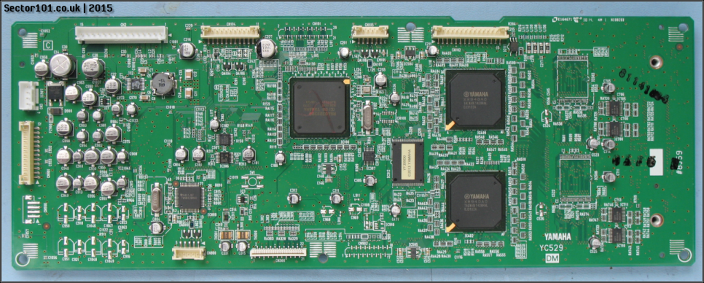
The photo below shows the Top Side of the DM PCB. This is where all the sound processing is done

This seems like a standard modern PCB design. SMD components are used throughout (except a few connectors). The Main Processor & 2x Voice ICs are in space-saving BGA format. The Firmware I guess lives in the TSSOP-56 IC with the little yellow label on it “YF3990 (c) 2013 YAMAHA”
What does catch the attention are the unpopulated areas of the PCB. To the left there is a non-fitted connector CN900, and an array of capacitors missing similar to the pattern of capacitors above it. Move along to the bottom center and C902 is missing along with some support circuitry nearby. At the top center CN101 is missing. Keep going right and there are 2x TSSOP-56 package layouts non-populated as well. These two component layouts almost beg the question “was on-board Flash ROM storage considered at the design stage..?”
The photo below shows the Bottom Side of the DM PCB.

To the left you have the Flash Board connector, buffers, and the two onboard WaveROM ICs in TSSOP-56 fromat. The two unpopulated TSSOP-56 layouts on the top side are directly underneath these WaveROM ICs. Near the center there are two TSOPII-54 ICs which are probably SDRAM used as workspace for the 2x Voice ICs on the top side. Further right there are another 2x TSOPII-54 ICs – again probably SDRAM used as workspace for the main CPU.
There is an unpopulated area at the bottom right of the PCB which suggests another DAC & Amp circuit could be fitted (for more Outputs..?). The missing cluster of capacitors on the top side are underneath this area.
The JK PCB
The photo below shows the Top Side of the JK PCB.

This is a single-sided populated board. Components on the top, traces on the bottom, all thru-hole components.
The bottom row of connectors on this PCB (from left to right) are:
- MIDI: Thru, Out, In
- Foot Switch – Assignable
- Foot Switch – Sustain
- Foot Controller
- Output: Right, Left
- Phones
- A/D Input: Right, Left
The KEY-IF PCB
The photo below shows the Top Side of the KEY-IF PCB.

This PCB connects to the keybed so it scans the keys and probably calculates the velocity as well. Mostly an SMD PCB, single sided.
This particular PCB has suffered at the hands of a clumsy assembly operator. It appears when the operator was driving in the screw at the top-left it missed the hole in the PCB and travelled across the PCB whilst the driver was still rotating. Closer inspection show that this happened at least three times before being successful. Thankfully the board still works😐
The LCD PCB
The photo below shows the LCD PCB mounted in the top casing.

There’s a large area on the right of this PCB unpopulated – maybe this is the circuit for a ‘touch-screen’ version of the display..?
The PS PCB
The photo below shows the PS PCB.

A single-sided PCB with mixed SMD and thru-hole components.
The Wall Wart adaptor plugs into this and the power is distributed around the MOXF6 hardware.
The USB PCB
The photo below shows the USB PCB.

This is the “To Device” & “To Host” PCB. Again a single-sided PCB with mixed SMD and thru-hole components.
The Keyboard
The photo below shows how the keys are held in place.

The keybed shows where costs have been trimmed down. On the older SY series each key was a separate component that can be removed & replaced if needed.
On the MOXF the black keys are in groups of five on the same strip and the white keys are in groups of seven. This simple assembly allows the keys, key pivots and anchor points to be part of the same plastic molding. Downside is that if you break a key then you need to get all 5 or 7 depending on black or white.
Test Menu
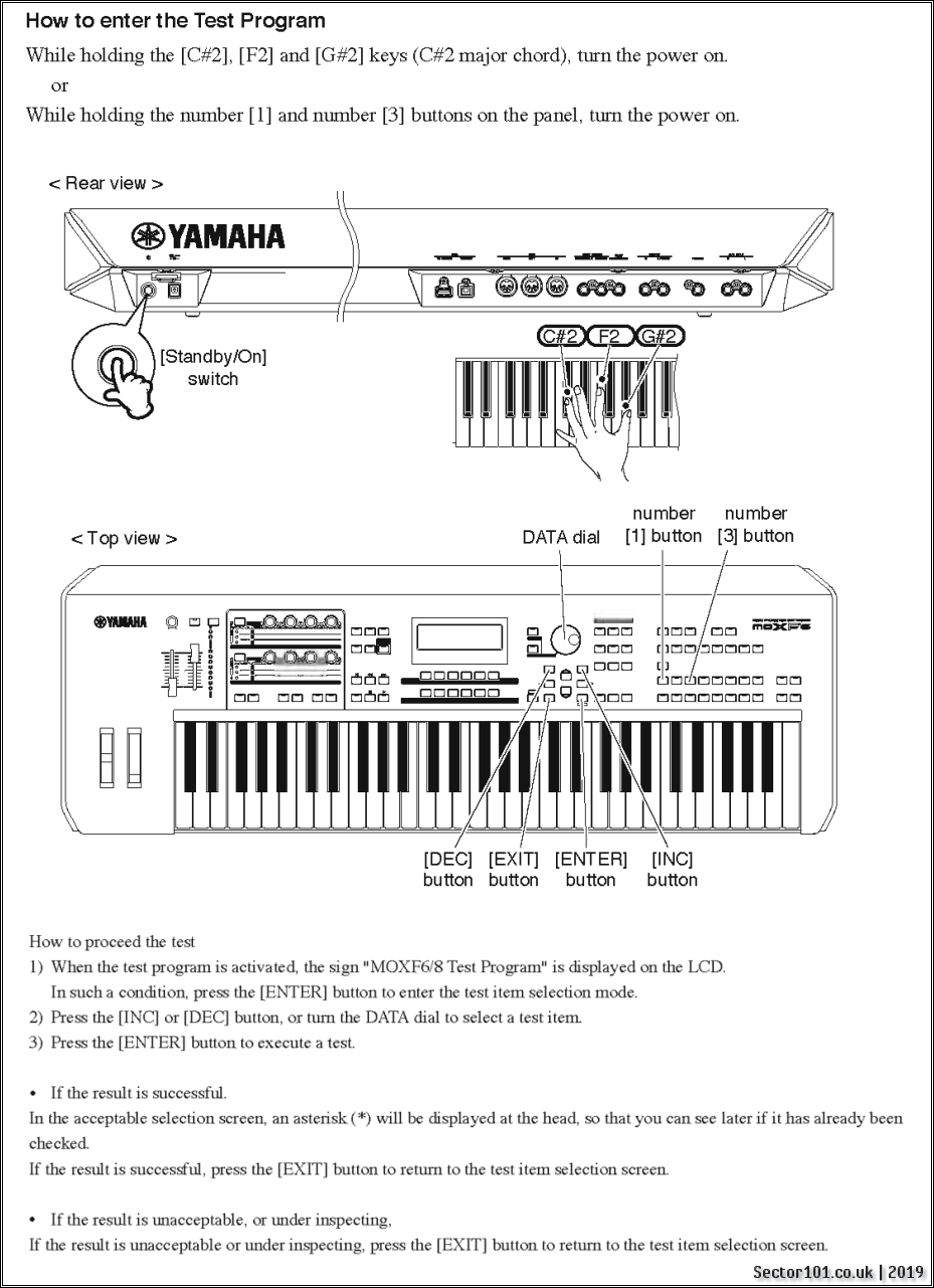
The MOXF has a diagnostic test menu that can be activated by holding down certain keys whilst powering the unit on.
Please see the instructions below on how to activate the tests:


// END
Hi Brian! I recently purchased an used Yamaha MX49, its like a “mini” version of this keyboard, but the FX RAM its faulty and I can’t use any FX process on this synth 🙁 I ran the test mode and it indicates that FX RAM 1 and FX RAM 2 are “NG”. I need your help for trying to figure out which ICs are involved on this, please. I can send you pictures of the PCB. Have a good night!
Hello,
Without the Service Manual I cannot give an accurate answer to your query. I tried looking for the service manual but got nothing.
The NG test result does not give any useful information. It is unlikely that both FX RAM ICs are bad, the problem could be the effects processor itself, or solder connections on the PCB.
Hi again, thanks for your reply!. I asked for the service manual to Yamaha Support Center, and they sent it to me. Here’s the link: http://www.yamaha.com/yamahavgn/Service_Manual/Service/Synthesizer/MX61_MX49_C%5B1%5D.pdf
There appears to be two tests for effects:
o On page 31 of the manual there is Test No. 005
o On page 35 there is Test No. 032.
What are the results for both these tests?
In the schematic I see IC 202 as the DSP (Effects) Memory. This is a W9864G6JH-6 SDRAM device.
The W9864G6JH-6 SDRAM is now obsolete so cannot be bought through normal vendors.
Alliance make a compatible SDRAM – AS4C4M16S-6TCN.
Mouser stock this item here:
https://www.mouser.co.uk/ProductDetail/Alliance-Memory/AS4C4M16S-6TCN?qs=%2Fha2pyFaduhsSHb9Rb%252BxlnALafqFQ9ezA3ifNoAzNsx%2FrcjioeyTVQ%3D%3D
The results for both test are: NG (that’s the opposite of OK, I assume). So maybe IC 202 failed or there is a bad solder connection, thanks for the info!. Btw, sometimes I think that maybe is related to firmware issues, such as a bad firmware update attempt, is it possible?